By Paul Evancoe
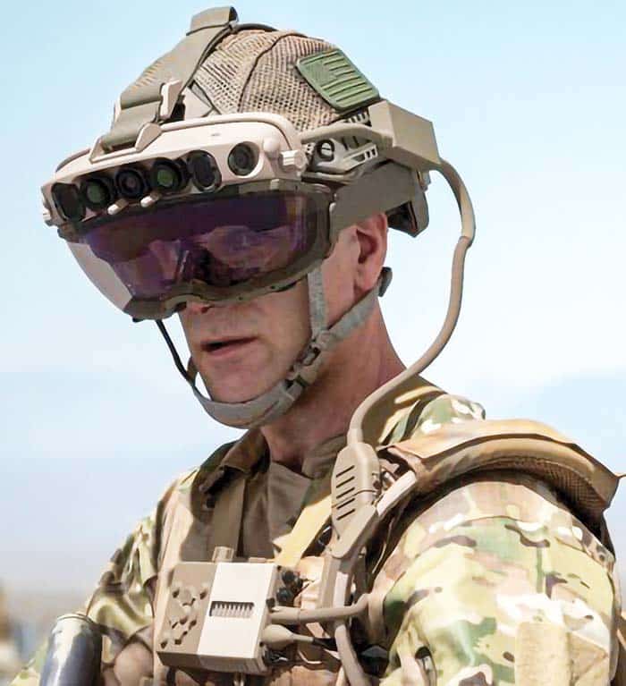
The optical sighting device industry is heading toward replacing traditional ground lens see-through glass optics with optoelectronic sighting devices. This evolution is made even more potent through the integration of optoelectronics and artificial intelligence (AI). Like high definition multi-spectral cameras and viewing screens that offer reliable performance under all light extremes and environmental conditions, sophisticated technology is slowly becoming the norm. For example, the U.S. Army’s Program Executive Office Command, Control, Communications-Tactical seeks single-channel data radios that can “support and integrate” with the Integrated Visual Augmentation System (IVAS). The IVAS program, led by the Soldier Lethality Cross-Functional Team, provides soldiers with artificial intelligence—enhanced goggles that assist with navigation, targeting and advanced night and thermal vision (more on this later). Will this technology transition to the sporting firearms market? Absolutely! It already is.
Perhaps a quick review of the technology may be helpful. Optoelectronics is the science and application of electronic devices that source, detect and control light. Many consider it a sub-field of photonics (the science of radiant energy). In this context, light includes visible light and invisible forms of radiation such as gamma rays, X-rays, ultraviolet and infrared. Photonic devices are electrical-to-optical or optical-to-electrical transducers (devices that convert forms of energy) or instruments that use such tools in their operation. Electro-optics is often erroneously used as a synonym for optoelectronics. While related, “electro-optics” encompasses a much broader physics branch that includes all interactions between light and electric fields, whether or not they form part of a particular electronic device.

Remarkably, optoelectronics is not a new technology. It can be traced back to 1907 when Englishman Henry Round (remember this name) discovered electroluminescence using silicon carbide and a cat whisker while experimenting with a turn-of-the-century crystal radio set.Uniquely, this straightforward radio receiver’s only source of power comes solely from the power of radio waves received via its long-wire antenna. It gets its name from its most crucial component known as a crystal detector, originally made from a piece of crystalline mineral such as galena.
Galena is the naturally occurring ore of lead. Galena crystals act as a semiconductor with a small bandgap of about 0.4 eV. In solid-state physics, a bandgap (also called an energy gap) defines an energy range in a solid where no electron states can exist. In graphs of the electronic band structure of solids, the bandgap refers to the energy difference (in electron volts, expressed as eV) between the top of the valence band and the bottom of the conduction band in insulators and semiconductors. Valence refers to an electron of an atom, located in the outermost shell (valence shell) of the atom, that can be transferred to, or shared with, another atom. Therefore, the bandgap is a significant factor determining the electrical conductivity of a solid. Substances with large bandgaps are generally insulators; those with smaller band gaps are semiconductors, while conductors have very small bandgaps (or nearly none at all) because the valence and conduction bands overlap.

First crystal radio sets used galena crystal as a point-contact diode capable of rectifying alternating voltages and current and detecting radio signals. The crystal was “tuned” with a sharp-pointed wire, known as a “cat’s whisker.” The radio’s operation required that the point of the wire in contact with the galena crystal be shifted about the crystal’s faceted surfaces to find a part of the crystal that acted as a rectifying diode. Today the crystal and cat whisker has been eliminated, and this component is called a diode. Diodes are manufactured with specific purpose-intended semi-conductance values. Semiconductors are the foundation of all modern electronics because anything that’s computerized, like AI or optoelectronics, relies on semiconductors.
Understanding the properties of a semiconductor relies on quantum mechanics to explain electrons’ movement through holes in a crystal lattice.The development of the first transistor in 1947 was made possible by Albert Einstein’s development of quantum mechanics theory. Yet, the path from Einstein’s ingenious quantum mechanics theory to the first manufactured transistor involved thousands of science and engineering hours, numerous failed attempts and billions of dollars. In other words, it was neither easy nor cheap.
Today’s semiconductors are made from material with an electrical conductivity value falling between a conductor, like copper, and an insulator, such as silicon (glass). Therefore, something in-between qualifies as a semiconductor. Semiconducting material exists in two types: elemental materials (pure metals: e.g., gold, silver, copper, etc.) and compound materials (alloys). Using compound materials provides a means to “tweak” the metal’s semiconductive properties (band gap) to achieve a particular component’s purpose. Semiconductors are at the heart of microprocessor chips, as well as transistors.
In the 1920s, Russian physicist Oleg Losev further advanced Henry Round’s electroluminescence research. Losev studied the distinctive properties of light-emitting diodes (LED) in radio sets and published several detailed scientific papers that quantified and documented his findings. Even though one might assume World War II’s wartime necessity would have furthered Losev’s research, it was largely overlooked until the late 1950s. Remarkably, history can’t provide a reason. Whether the scientific community simply didn’t realize the potential or whether LEDs were misunderstood remains a mystery.

In early 1961 while creating a laser diode, Bob Biard and Gary Pittman accidentally discovered the infrared light-emitting diode (LED) at Texas Instruments. In 1962, General Electric’s Dr. Nick Holonyak, Jr. developed the first visible red light LED. This development led the future discoveries of multi-colored LEDs, liquid crystal diodes (LCDs), organic LEDs (OLED) and made possible the expansion of optoelectronics. Applied variations of these diodes are incorporated in every optoelectronic device made today. From smartphone cameras, computers of all kinds and sizes, visible and IR spotting and ranging lasers, low light imaging devices, starlight-magnifying devices, passive and active infrared sighting and imaging devices, to HD digital multi-spectral micro-imaging, flat-screen monitors, high-intensity visible light LED light bulbs, flashlights, headlights, marker lights—the optoelectronic device list goes on and on.
The future for optoelectronics is bright (no pun intended). We are witnessing the exponential advancement of the computing power necessary to enable the marriage of artificial intelligence and optoelectronics. This makes possible the incorporation of features like instantaneous imaging analysis, navigation, ranging, all-weather day/night and spotting capabilities, a user heads-up display (goggles or visor), an encrypted data recording capability, an encrypted data-in-motion link to any smartphone for real-time social media-like or other communications connectivity and the uploading/downloading of updates and data, to name a few.
We are witnessing the exponential advancement of the computing power necessary to enable the marriage of artificial intelligence and optoelectronics.
AI-augmented optoelectronic devices include real-time image identification capabilities, target acquisition and classification, electronic picture stabilization, clutter reduction and/or elimination and a host of other effectiveness options that instantly manipulate, integrate and interoperate image data, target I.D. and firing solution and present it in an understandable intuitive, user-friendly format. At some point these devices will be cheaper to manufacture than traditional glass optics, smaller and lighter to carry, more rugged with a longer life expectancy and provide downloadable, upgradeable, fully-programmable capability with apps all in one AI-augmented optoelectronic multipurpose sight. Remarkably, this technology currently exists. It’s a matter of functionally combining it in a cost-effective package.
So why aren’t manufacturers offering the ultimate gun sight that includes some or all of this technology? The answer is simple. It is available, but it’s expensive. Manufacturers are slowly adding optoelectronic capabilities to their product lines. However, with the addition of sophisticated technology comes the inherent problem of user interface, training and familiarity. The analogy is similar to problems designers faced when teaching pilots to fly a drone. The engineers quickly realized that it was easier to train a computer game player to fly a drone using a game-like hand paddle and joystick than by using something that simulated an aircraft cockpit. The reason was user familiarity (muscle memory).
Most of today’s generation grew up playing computer games and they are at home with the gaming controls that all operate similarly. So, the transition to drone piloting using similar functioning game-like controls is logically straightforward. That is precisely the challenge optoelectronic device design engineers now face. They must design sophisticated devices with controls that closely mimic something that the users are already familiar with and know how to use. Like the drone controllers, the optoelectronic gun sight controls must look, work and feel much the same no matter what brand they carry. AI can help with this by operating most of the technically sophisticated tasks involved without the user even realizing it’s being done for him or her. But there is another concern that goes hand-in-hand with sophisticated AI operations—and that is one of user trust.
So why aren’t manufacturers offering the ultimate gun sight that includes some or all of this technology? The answer is simple. It is available, but it’s expensive.
Trust is necessary when AI is involved in the decision process. For example, things like AI target ID followed by instantaneous engagement requires user trust. Even more so if the AI is autonomously empowered to engage the target without human permission. The problem faced in this scenario is that AI operates at light speed and humans do not. If human permission is required in the AI decision loop (lacking full trust in AI making the correct decision), it will serve to severely slow the process, if not confound it. If a target image has to be transmitted for a human to look at it (evaluate) and then decide to push the “fire” button, that is an eternity at the speed AI operates at. The resulting lag seriously jeopardizes winning the fight. So it logically follows that an AI that has to get human approval to shoot will always be beaten to the draw by an AI that doesn’t. The good news is this problem can be overcome with sufficient AI-human trust. The bad news is the manufacturers aren’t yet working toward a common trust-based operating baseline.
There is always a downside to most things that appear almost too good to be true. In this case the penalty involves the Law of Physics consisting of two major obstacles, thermal fluctuations and random quantum fluctuations—a barrier known as the standard quantum limit. As AI-augmented optoelectronic devices become more powerful, so does the requirement for power and power equates to entropy. Additionally, the standard quantum limit for the noise of an optoelectronic device refers to the minimum level of quantum noise which can be obtained without the use of squeezed states of light (very pure vacuum-enhanced states of light with minimal noise). This translates to unavoidable noise distortion in optical amplifiers resulting from the spontaneous emission of excited atoms or ions. It’s somewhat analogous to the static one hears when a powerful amplifier is turned up to its maximum amplitude. It’s a problem that DARPA has been working on for a number of years and may never fully resolve.
DARPA is also working on the ability to automate the processing, exploitation and dissemination of massive amounts of full-motion optoelectronic imagery (“big data”) collected by U.S. and allied intelligence, surveillance and reconnaissance (ISR) assets in operational areas around the globe, using AI as a discriminator. The sheer volume of this raw imagery intelligence is impossible for human analysts to sort through, much less analyze and correlate, making AI analysis a necessity.
Following the 2011 U.S. withdrawal from Iraq, the Department of Defense (DoD) set its sights to adapt its warfighting tools and strategy for the next decade. Designated Project Maven, the DoD’s central focus is the employment of artificial intelligence (AI) and machine learning (ML) in the global fight against terrorism. Machine learning relies on the statistic that, in any large set of data, there will emerge clusters of data points that correspond to things in the real world and this data volume requires AI “deep learning.”

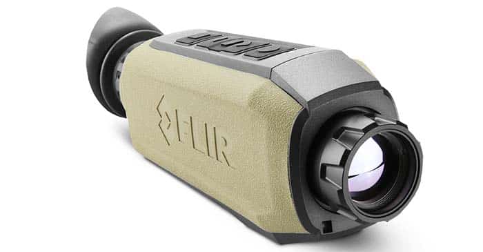
We mostly understand what AI and machine learning is, but what is deep learning (DL)? As the company FLIR explains it:
… deep learning is a form of machine learning that uses neural networks with many “deep” layers between the input and output nodes. By training a network on a large data set, a model is created that can be used to make accurate predictions based on input data. In neural networks used for deep learning, each layer’s output is fed forward to the input of the next layer. The model is optimized iteratively by changing the weights (values) of the connections between layers. On each cycle, feedback on the accuracy of the model’s predictions is used to guide changes in the connection weighting.
Traditional smart cameras combine a machine vision (optoelectronic) camera and a single-board computer running rules-based image processing software. This provides a great solution for simple problems like barcode reading or answering questions like “On this part, is the hole where it’s supposed to be?” Inference cameras excel at more complex or subjective questions like “Is this an export-grade peach?” When trained using known good (reference) images, inference cameras can easily identify unexpected defects that would not be recognized by rules-based inspection systems, making them far more tolerant to variability.
Inference cameras can be used to augment existing applications with rich, descriptive metadata. For example, these cameras can use inference to tag images which are passed to a host that carries out traditional rules-based image processing. In this way, users can quickly expand the capabilities of their existing [optoelectronic] vision systems.
This hybrid system architecture can also be used to trigger a traditional vision system for human viewing.
The combination of AI-augmented optoelectronics and ML running specialized DL algorithms designed to search for, identify, correlate and categorize specific items (even people) of interest in massive volumes of data is the future. Project Maven’s initial results in successfully exploiting “big data” by operationalizing AI/ML indicates DoD is transitioning from its historic hardware-centric organization to one that is AI/ML data-driven.
Another underway example (mentioned earlier) is the U.S. Army’s Integrated Visual Augmentation System (IVAS). IVAS consists of an optoelectronic Heads-Up Display (HUD) helmet-worn visor that will allow soldiers to experience AI-augmented reality. The IVAS includes an optoelectronic HUD, a body-worn computer and networked real-time communications and AI-capable data connectivity. The IVAS uses various optoelectronic imaging sensors, artificial intelligence and machine learning to provide a fully integrated day/night combat capability at the forward edge of the battlefield. It will be fully integrated into combined combat operations to increase lethality, mobility and soldier situational awareness. It will also enable soldiers to train in synthetic environments with the same equipment they use in combat.
Like high definition multi-spectral cameras and viewing screens that offer reliable performance under all light extremes and environmental conditions, sophisticated technology is slowly becoming the norm.
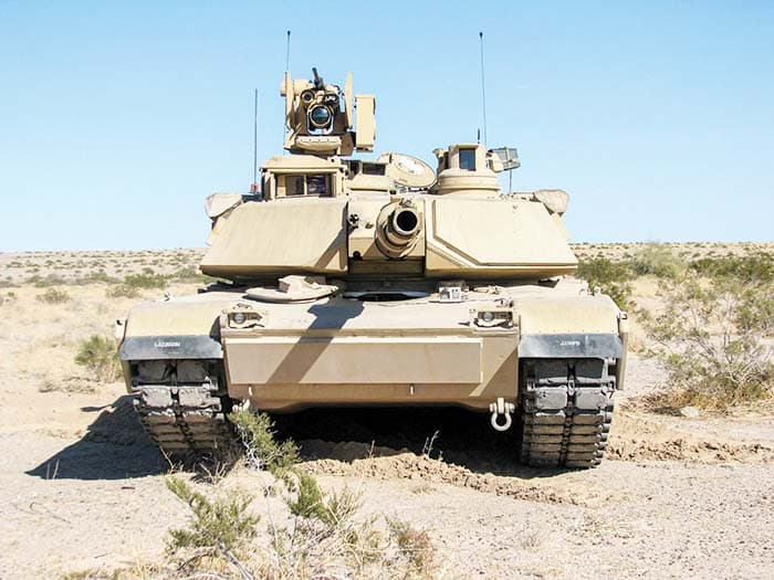
Another similar program along the lines of IVAS (but on steroids) is an AI/optoelectronic upgrade to the M1 Abrams tank’s sensor suite, target display, tracking and fire control systems, and ability to provide and receive real-time targeting data to and from other tanks, and target designating sources like drones, spotter aircraft, ground units, etc. This system relies on optoelectronic eyes and AI targeting analysis and target prioritization. It’s no less than brilliant.
As this technology proliferates, one might imagine it will transition, at some point, to sighting devices tailored for the sporting firearms market. These devices could very well operate much like IVAS providing the hunter visor-worn real-time all-weather day/night information on terrain, range, bearing, target identification, target validation and firing solution. It could even be augmented with safety information that would alert a hunter of no fire safety zone vectors or other humans within his field of fire. It could also provide a synthetic training environment that a hunter could use for practice, hunt rehearsal or hunt replay. Consider this feature for competition shooters.
AI-augmented optoelectronic gun sights for sporting purposes may never have mobile phones’ commodity status, so recovering development investments always results in expensive end cost products. Nonetheless, history reflects the profit impact of most technology evolution is still far greater than anticipated, mainly resulting from the related spinoff technology. As we proceed further into this decade, AI-augmented optoelectronics is becoming the mainstay of all space exploration and operations. Semi-autonomous robots already see with optoelectronic eyes and think using AI/DL. Spacecraft rely on this technology to navigate, image, analyze and classify physical surroundings. Fully autonomous robots will soon conduct specific tasks like site selection and then build human habitats in advance of humans on the Moon and Mars. We will likewise see them conducting fully autonomous mining of asteroids for precious minerals. We live in exciting times. Space (we used to say “the sky”) is the limit for the future of AI-augmented optoelectronics—imagine the possibilities.


